A Pictorial Tour of the Triple Wilson SVVCF Construction
At this writing (late May of 2010) I'm busily transferring this site from my old domain. This particular page brings back some vivid memories of the mother of all wiring jobs. People often mention how the Klee Sequencer is such a beast, but after wiring this module up, the Klee to me seems like a walk in the park.
As intense as it was, I don't regret it for a minute. This module remains one of my favorites, and, whenever I use it, it always contributes a bit of something that sounds at the same time wonderfully complex, yet organically appropriate. This is one of those modules that often reacts in profound ways to the most innocent of tweaks.
Anyway, since you're already here, you might as well scroll through the pics and get an idea how the lust for extraordinary functionality can also lead one to the brink of insanity. Or even over the brink, for that matter. If one is not careful, it can become very easy to paint oneself into a corner that can never be escaped....
 |
After my experimentation on the breadboard confirmed that this was a I place wanted to go, I ordered three SVVCF filter boards from MFOS.
 |
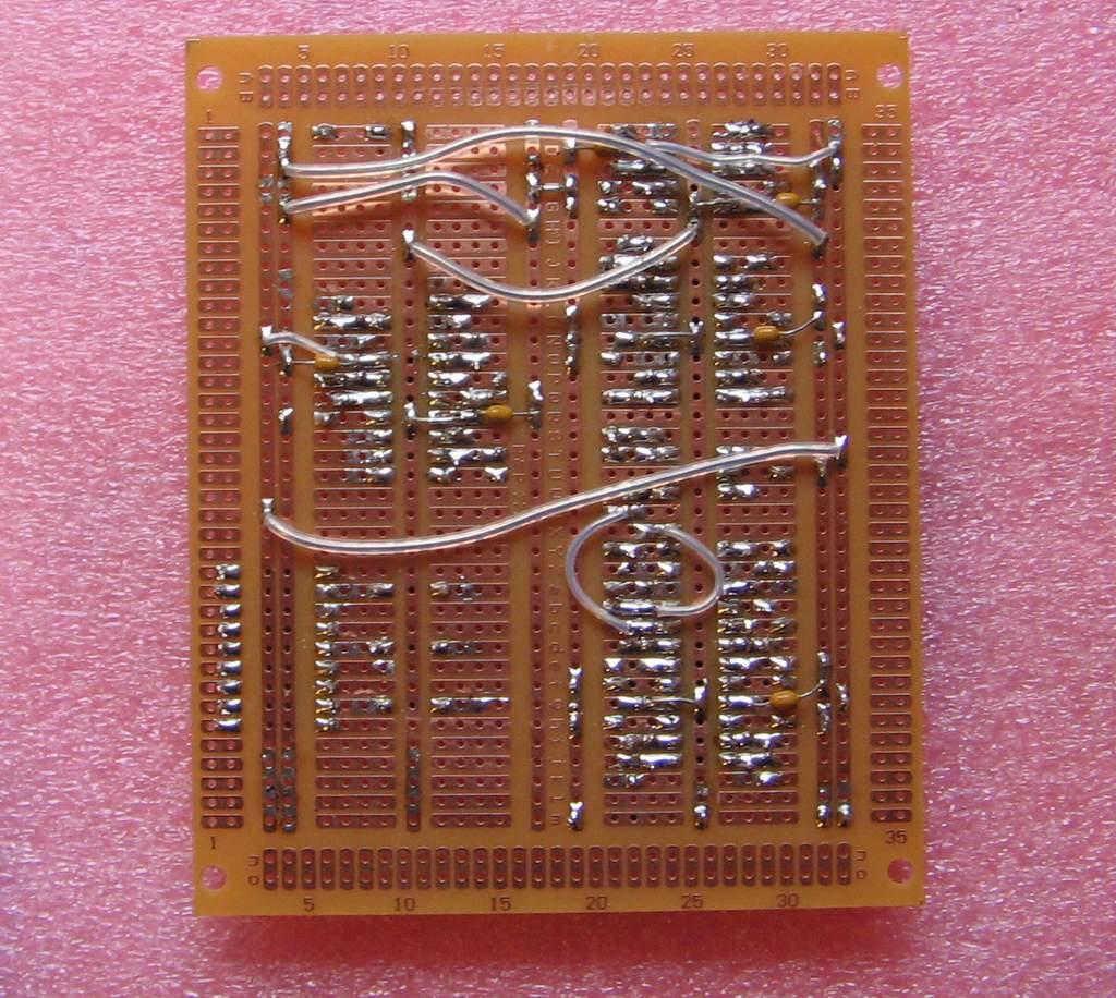
Stuffing the boards was a piece of cake. Notice I did not use all of the pads - each PCB needed only to handle one audio input, one CV input, one modulation input, one manual input and one resonance control input. The audio and control boards I designed would handle the mixing and inversion required to realize the functionality I required.
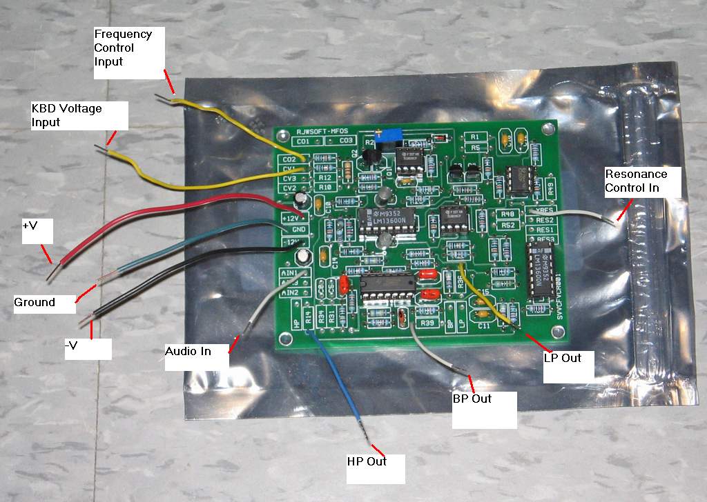 |
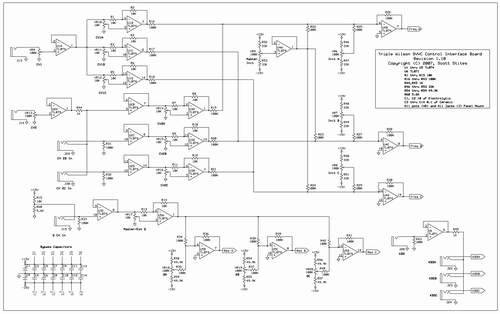
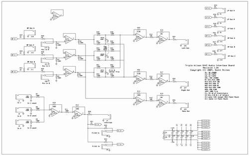
Here's a diagram of the connections I used for each board. As mentioned above, there is only one copy of each input designated for each board; each of the filter outputs is used. Also (of course) each board will require power and ground connections.
 |
After each board was stuffed, I tested each individually. In this picture, buried in the furry bit of wire in the middle of the picture is a single MFOS SVVCF undergoing test.
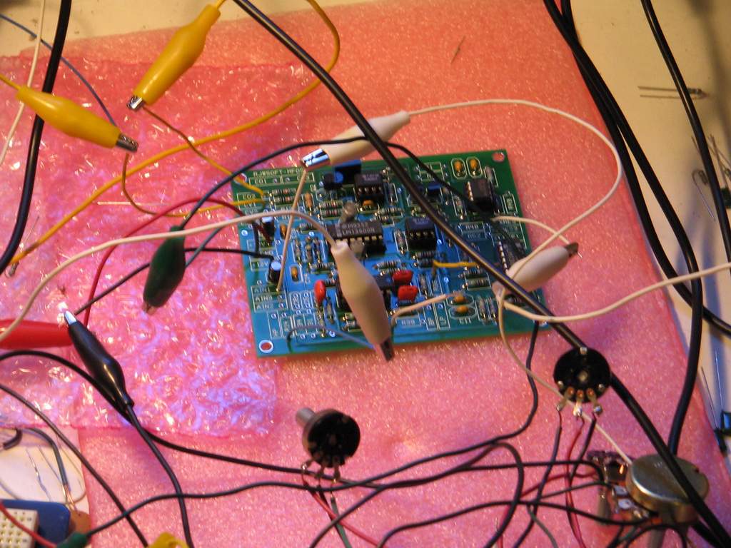 |
Here's a closer look at one of the MFOS boards hooked into the system through my usual medium of many-colored alligator clips.
 |
In order to implement the attenuation and inversion I required for the Triple Wilson SVVCF, I designed a control board to interface to each filter section. You can take a closer look by clicking on the pic - the link leads to a PDF of the schematic.
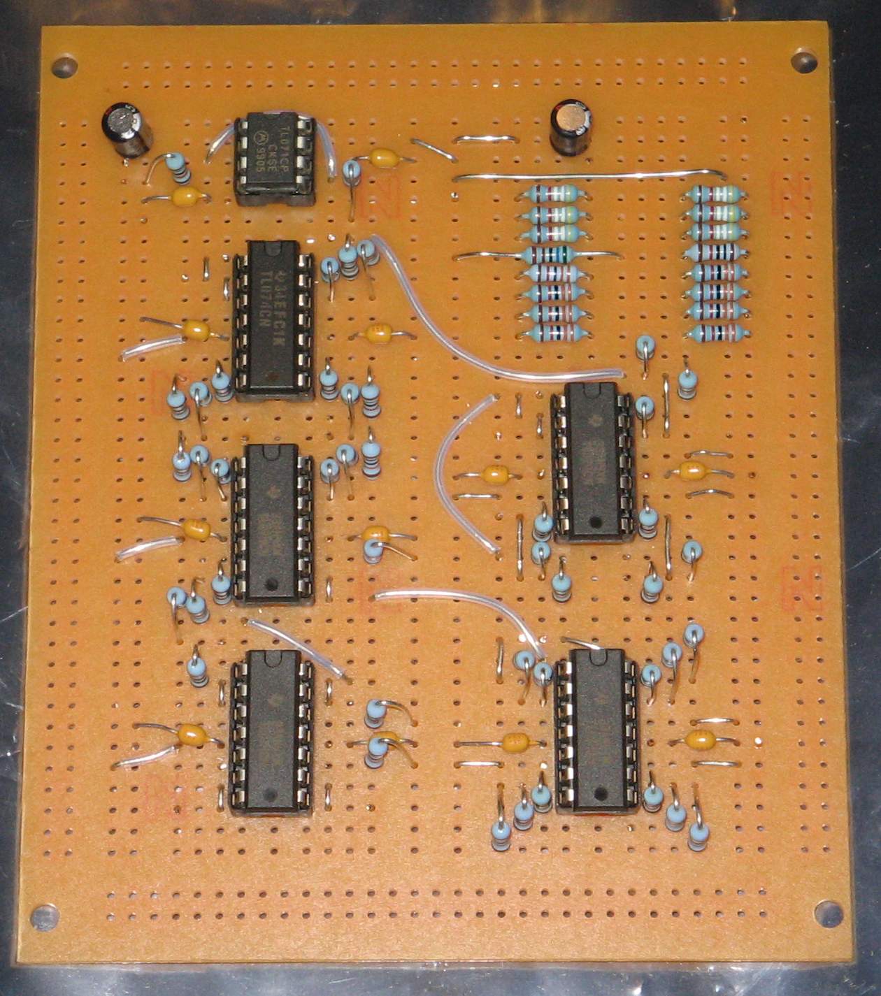 |
I built the control circuit using some prototype board that I purchased from Futurlec. As you can see from the pic and the schematic, it really isn't a terribly complicated circuit. The protoboard made it quite easy to build.
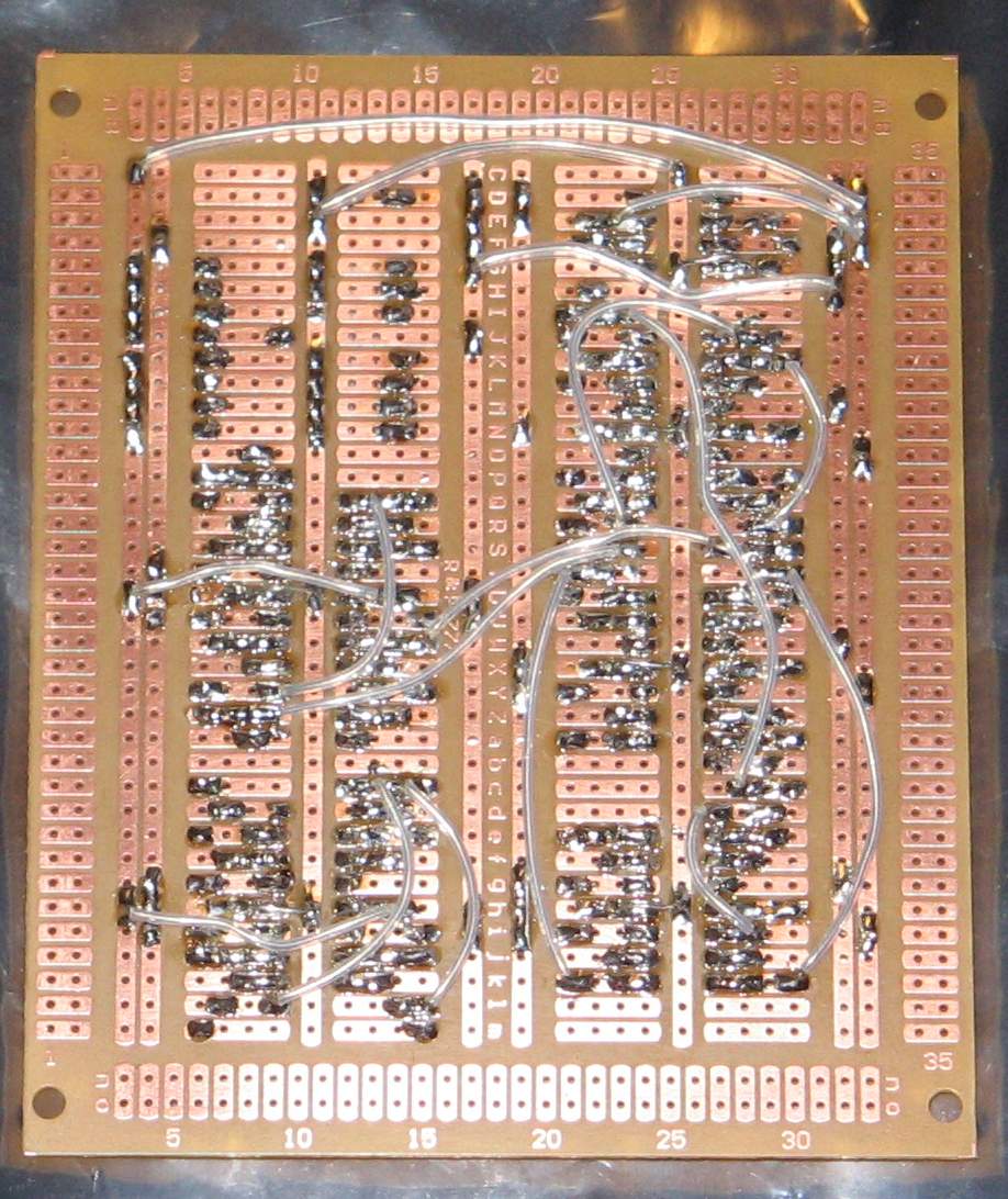 |
Here's a bottom (trace side) shot of the control board. The wire I used was just plain old bus wire using Teflon insulation, which (again) makes things pretty easy to build.
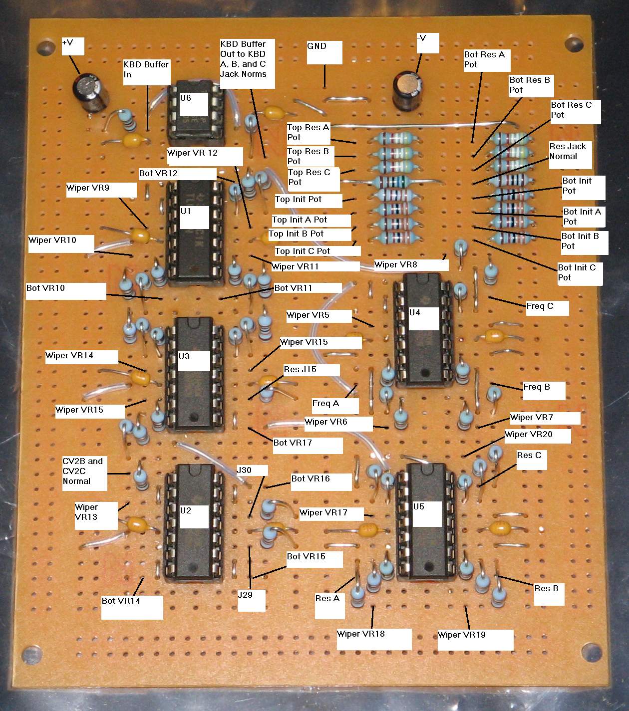 |
This is where the first glimmer of the true complexity of the module is revealed. This is a shot of the control board with the connection points labeled. Each label in this pic denotes a wire connection between it and the control surface (the panel), each of the three filter boards, and the power connections.
 |
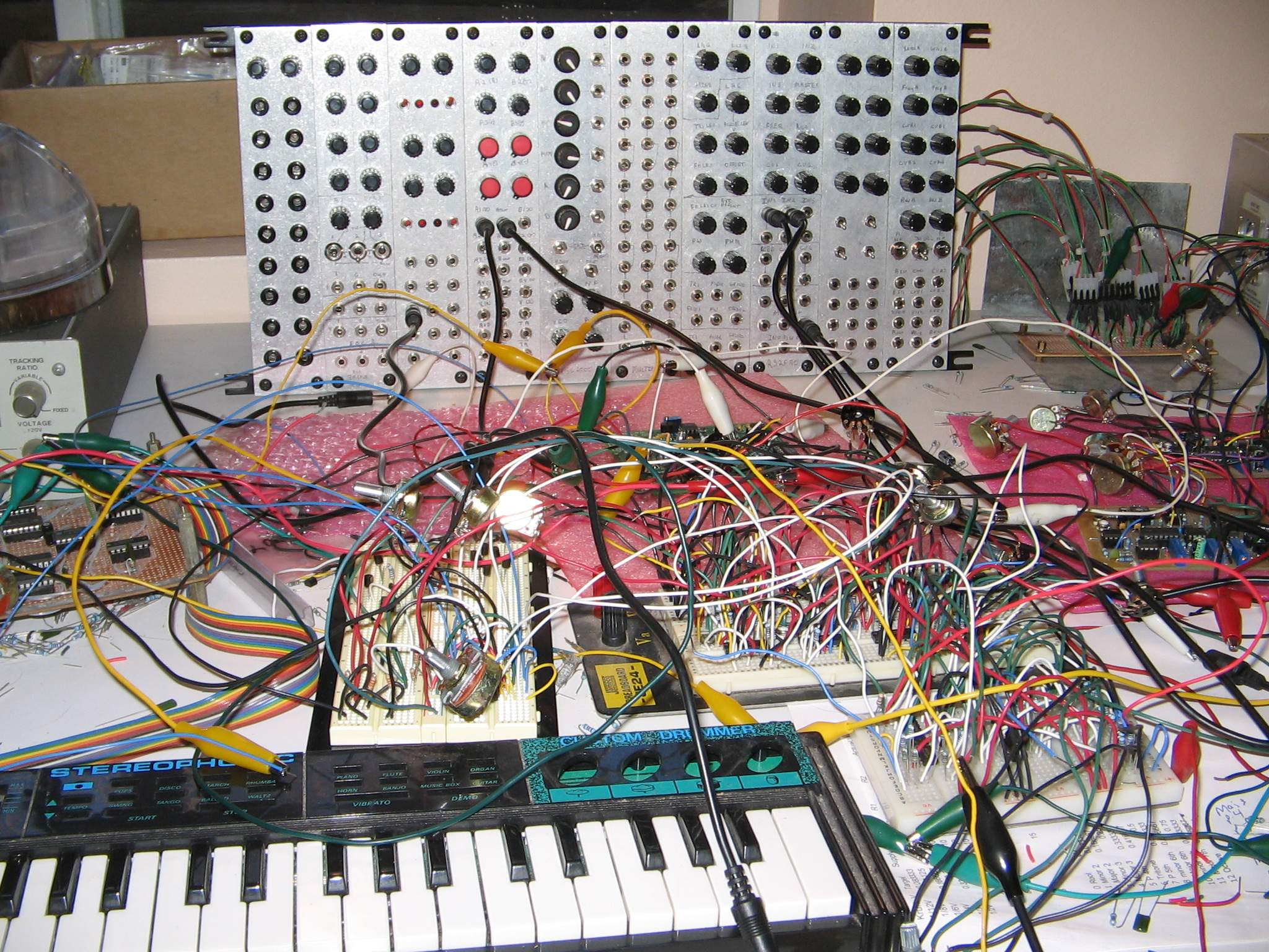
In order to test the integrity of the circuit, once the control board was built I soldered temporary solid core wires in all of the connection points of the control board. I then plugged those wires into breadboards which supported the pots that represented the front panel controls. I also connected straight to the MFOS boards through temporary wires soldered into them. The control board is rather obscured by all the wiring in this picture.
 |
Once the control board was confirmed to work as expected, I turned my attention to building the audio board. The audio board is used to mix the audio signals as well as provide equal power panning for the stereo output.
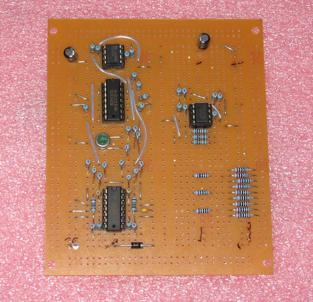 |
Once again a prototype PCB from Futurlec was used to construct the audio board. Four ICs and a handful of other parts, and it's ready to go.
 |
The backside of the board reveals that, like the control board, its not a terribly complicated circuit. Putting the bypass capacitors on the bottom of the board often helps to get a more immediate contact point on the supply pin of an IC.
 |
Like the control board, the audio board will be a very busy board when the time comes to wire everything up. Here the connection points are labeled for testing and final assembly.
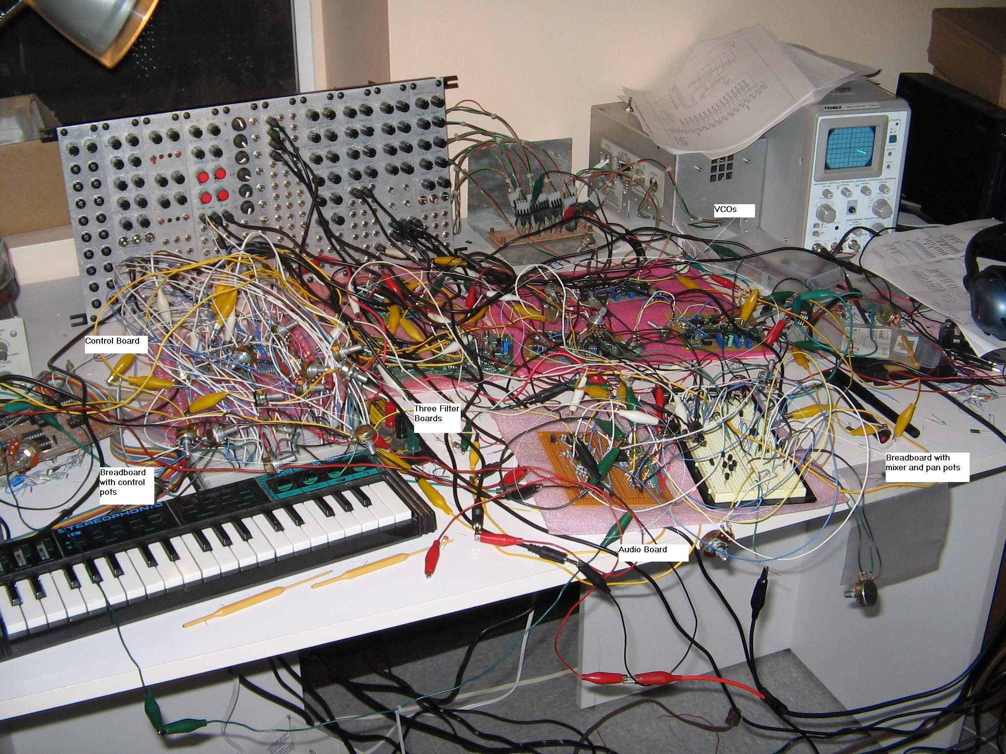 |
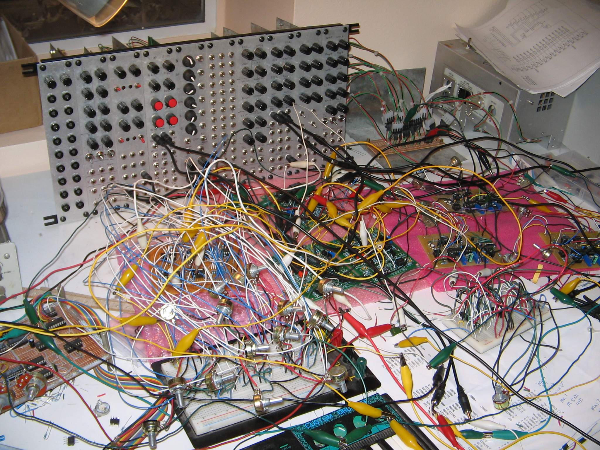
Here's a pic of the test apparatus used for testing the audio board, the control board and the three MFOS boards together. Right now, it's one hell of a strung-out module. It's time to make a proper synth module out of it.
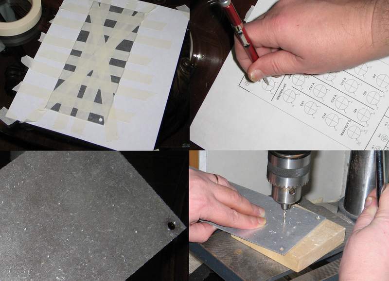 |
First up is fabricating the panel. A friend of mine chopped up some aluminum sheets I'd purchased into various sizes I envisioned my synthesizer would need. Here I tape the panel diagram to a blank panel. Then I center punch each hole that will be required on the front of the panel. After that, I drill very small pilot holes in the punch marks.
 |
Once the pilot holes have been drilled, I go after each hole with a stepped drill bit, being careful to make each hole the right size for the component that will mount into the hole. After the holes are drilled, I deburr them with a deburring bit.
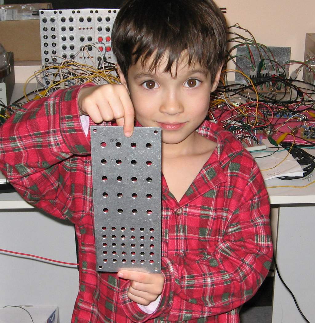 |
After several hours of painstaking work, my lab assistant Igor displays the finished drilled panel. Fancy sharpie scrawling will finish off the fresh home-made look at a later stage.
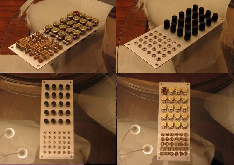 |
After the holes are drilled, I mount all of the components into the holes to make sure everything will fit. Everything fits. Barely.
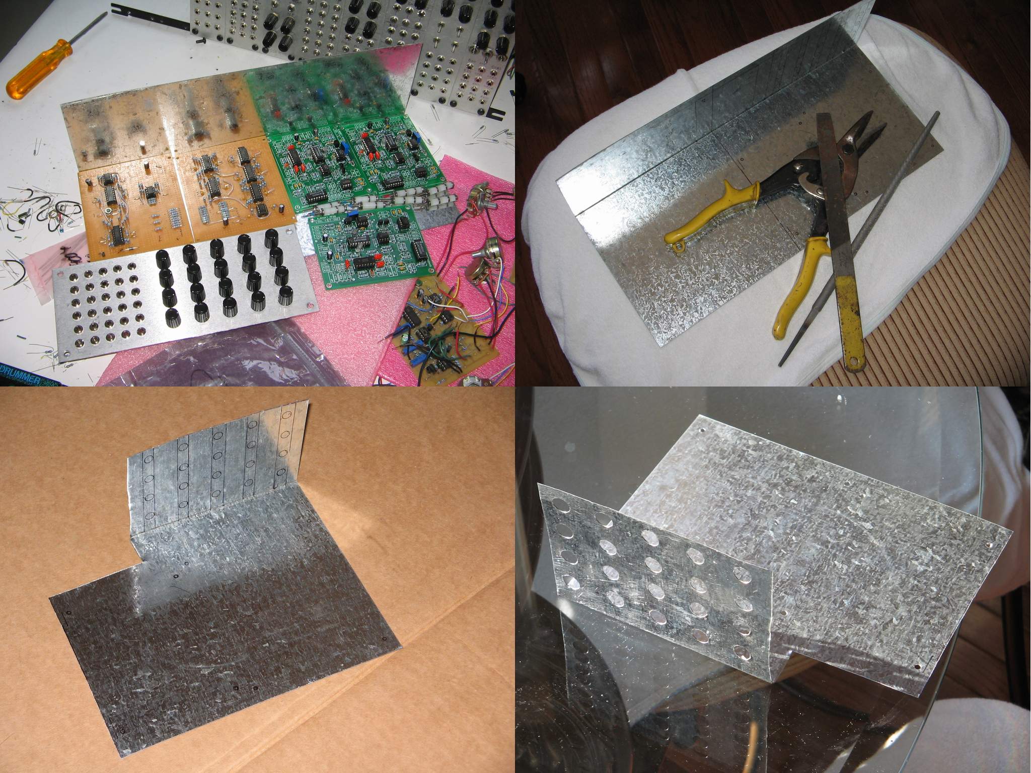 |
After the panel was finished, I needed to fashion a bracket that would attach the PCB to the panel. I use standard flashing material, which is pretty flimsy stuff when held horizontally. Mounted vertically (as it is mounted in my module) it is fairly sturdy. I would not recommend the material if you're building a gigging synth, however. Anyway, I mark the flashing with a sharpie using the front panel as a template. I mark the pot holes then where the flashing should cut away below the pots to allow room for wiring. Then I use metal shears to cut away the part of the flashing that needs to be removed. Then I drill holes where the pots will mount. I finish all of that off by filing down the cut edges of the flashing material so that it doesn't slice my fingers off when I pick up the module.
 |
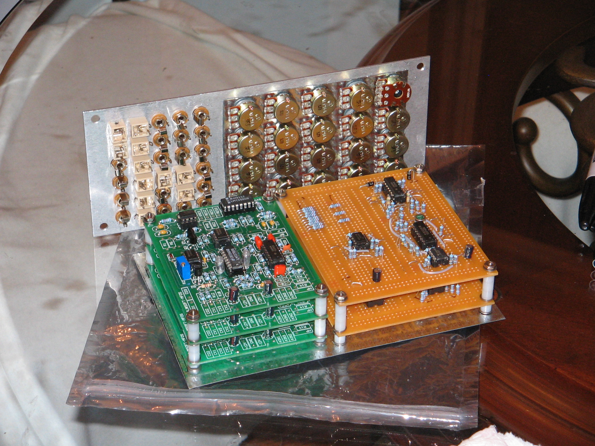
Once the bracket is done, I mark on the flashing material where the PCBs should mount on the flashing, then I drill holes for the PCB stand-offs. After that, I mount the PCBs to the bracket to make sure all five(!) PCBs will fit in the module.
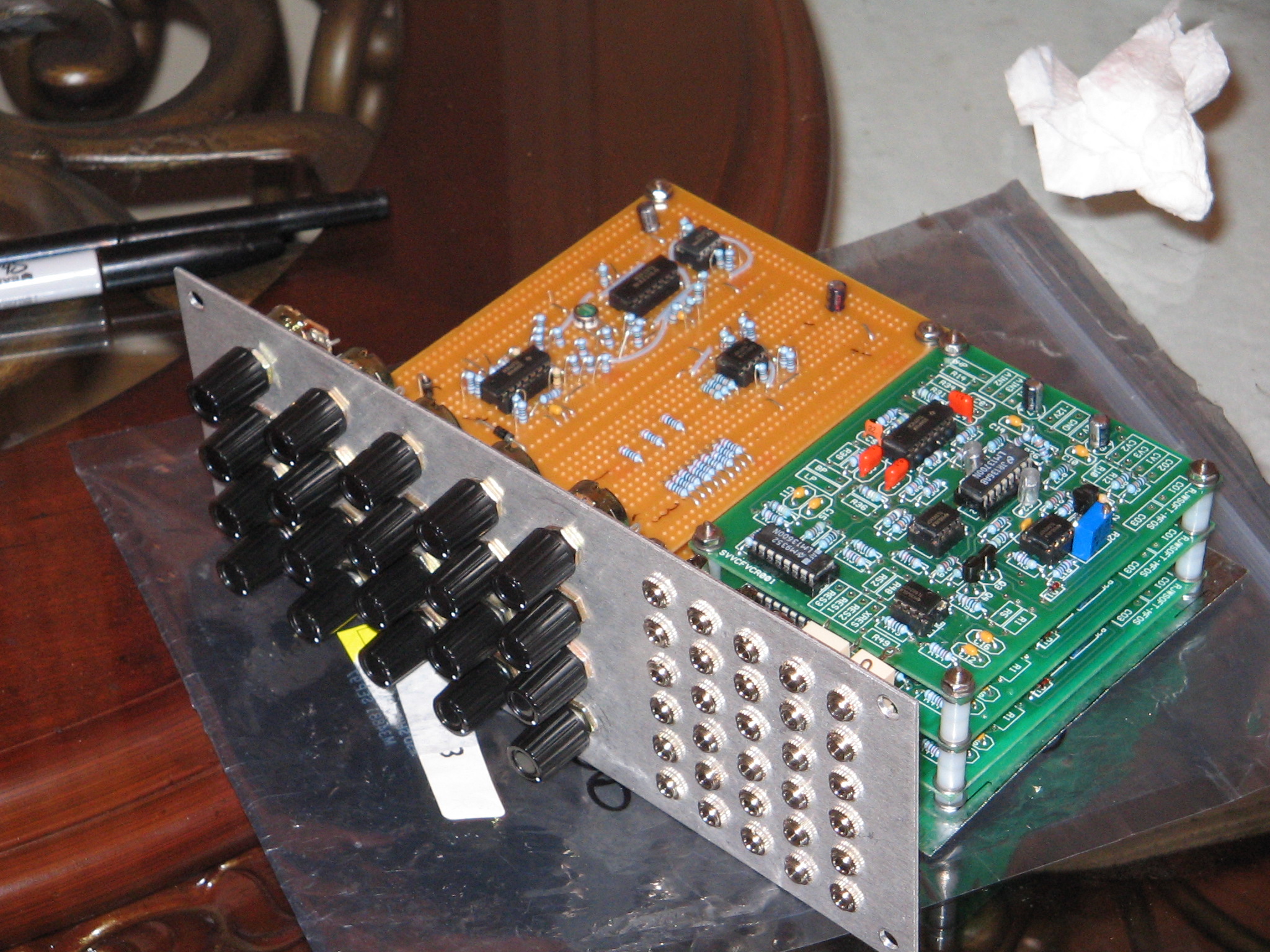 |
Once the PCBs are mounted on the bracket, I attach the bracket to the front panel, using pots to hold the bracket tight against the panel.
 |
Here's a rear shot of the mounted bracket/PCBs to the panel. You can see that I thread the pots through the holes cut on the flashing material and then tighten the pots down. This holds the PCBs tight to the module. The cut-away portion of the bracket allows access to wiring up the jacks.
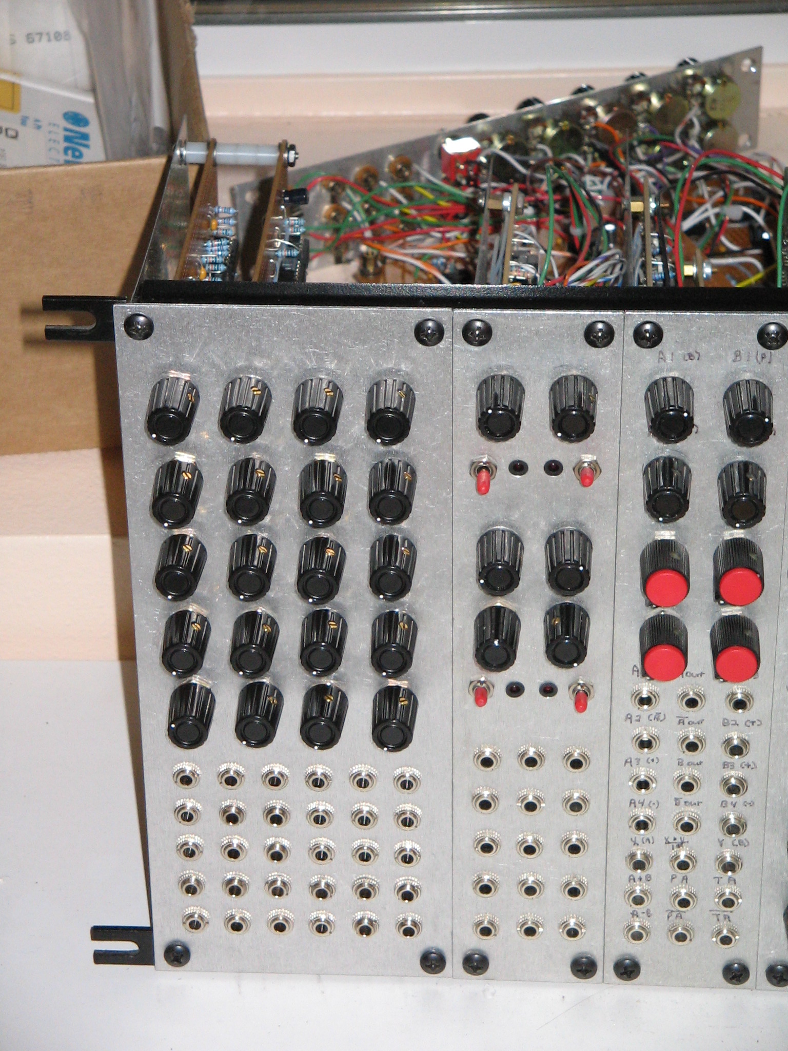 |
Just to be sure the module will fit in my synth, I mount the module in to see if the panel screw-holes align with the standard rack spacing that I use. Ahhh....fits like a glove. That leaves only the dreaded wiring as the final task.
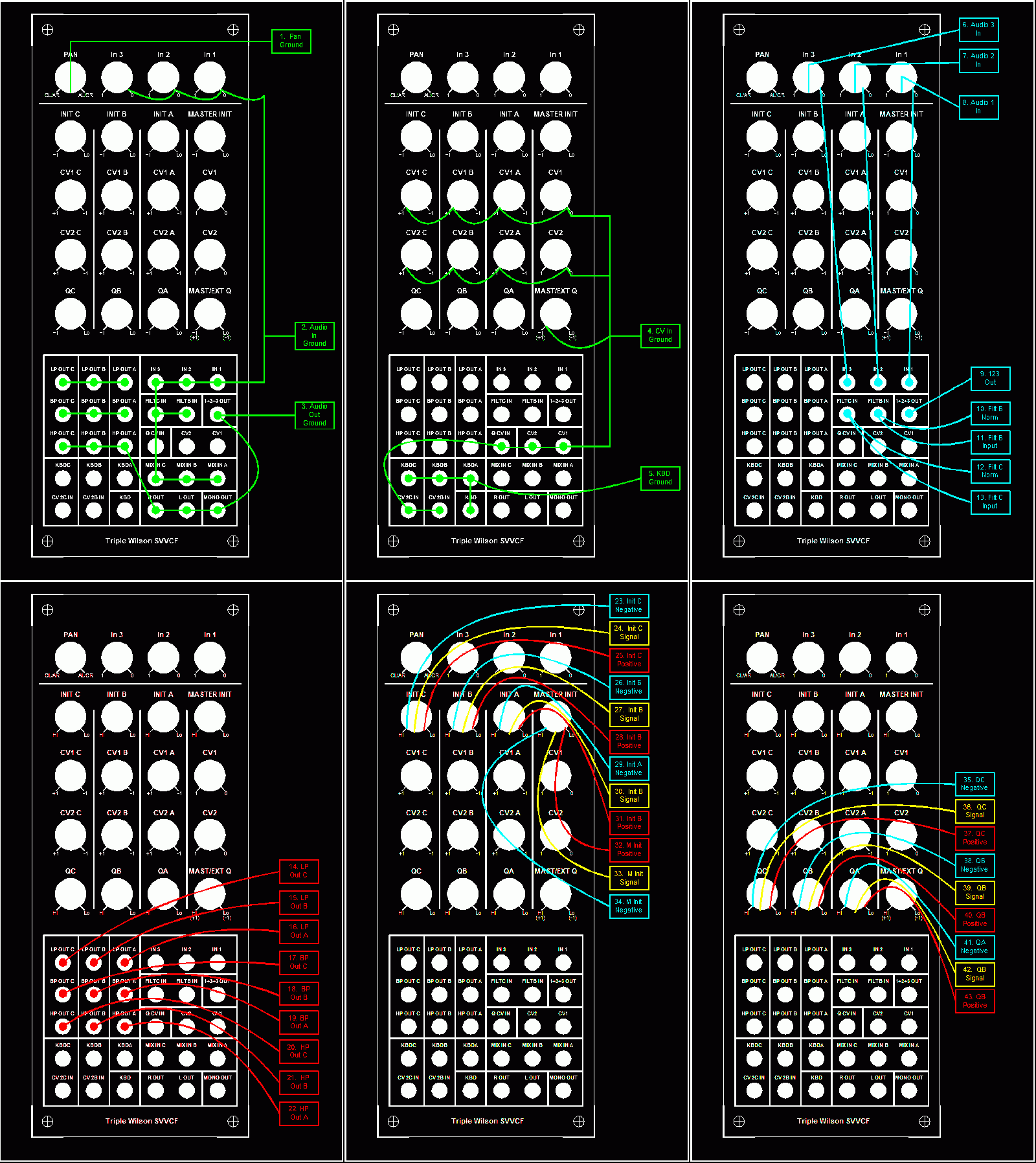 |
The wiring itself gets really complicated in a hurry. There are, after all, twenty pots (twenty one if you count the dual stereo pot) and thirty jacks to wire up to five different PC boards. In order to make sure that I wire everything up, and wire everything up correctly, I worked out some wiring diagrams for the module. I printed the panel in reverse so everything is referenced from the rear, since that is where all of the wiring will take place.
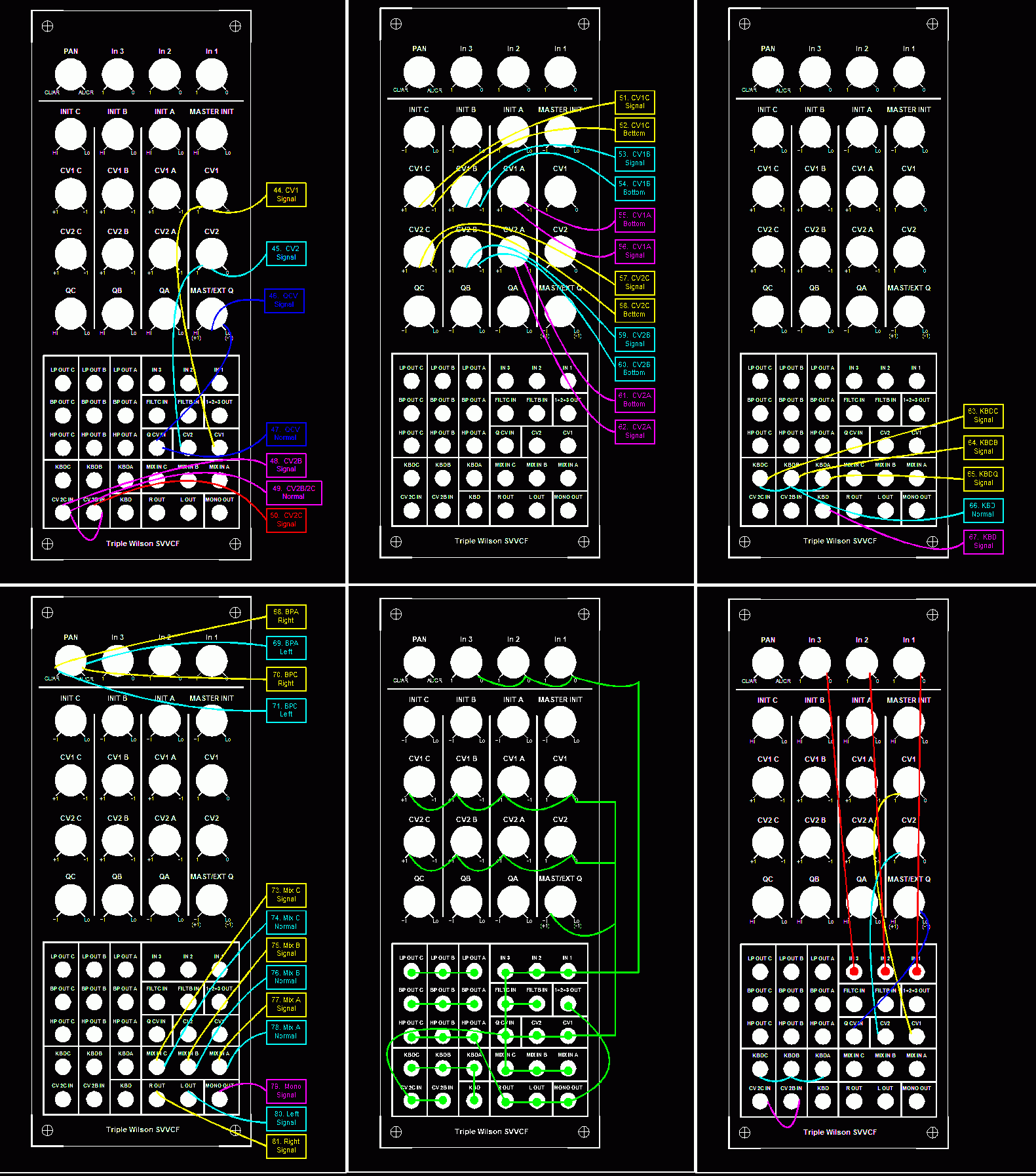 |
Each label on the above PCB pictures is accounted for in these drawings. Each line represents an individual wire that will need to be soldered into place.
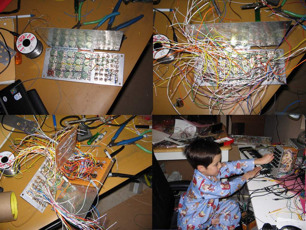 |
The wiring itself was a nightmarish three day ordeal. In fact, I was so engrossed in it, I didn't take a lot of pictures of the process. Let's just say it wasn't pretty, as is hinted at by the above picture. But, in the end, I think I only had one wire hooked to the wrong spot, and that was quickly taken care of. In the lower right you will see a picture of my lab assistant, Igor, running the finished module through its paces.