
The X-4046 VCO Project
A CD4046 Based VCO
As CMOS ICs go, one of the most compelling for us (and by "us" I mean synthesizer DIY geeks) would arguably be the CD4046. How can one resist the fact that this IC has not one, but two types of phase comparator built into it, along with an integral voltage controlled oscillator to boot? This is not your simple logic gate, multiplexer or shift register, but an IC with a combination of features one can really sink his teeth into.
Obviously the potential of using the CD4046 for musical applications has not been overlooked. For example, Scott Gravenhorst designed a great harmonic multiplier around the IC and the CD4046 forms an integral part of Grant Richter's famous Wiard Wogglebug.
Musical instrument designs based around the CD4046 tend to concentrate on the phase locked loop application the CD4046 was intended for in the first place. Most often, the 4046 is made to lock (however tightly or loosely) onto an incoming signal and produce the desired musical effect based upon the phase locked relationship with the external signal.
These applications, as well as others through the years, have proven to be very interesting and effective. However, what generally seems to be ignored is the usefulness of the VCO itself, and there is small wonder in that fact: in its native form, the VCO is a rather lackluster linerally controlled device that produces a pulse wave output. Why would one use a CD4046 as a VCO when a much simpler dedicated device such as a 555 timer can produce essentially the same results? Leave it to Thomas Henry to answer that question. Who would have supsected that by using a circuit that contains a mere four ICs and strategic manipulation of the IC itself, one could coax the following out of a CD4046:
Exponential Control and Modulation of the VCO
Linear Modulation of the VCO
Five unique waveform outputs (triangle, sawtooth, pulse (PWM), sine and variable rampoid
One of the finest hard sync effects ever heard from a VCO
Taking those features into account, the CD4046 VCO in itself suddenly becomes considerably more interesting.
The X-4046 VCO
As it turns out, the CD4046 VCO, under exponential control, can be a surprisingly compliant VCO, given that the CD4046, in all likelihood, wasn't designed with the intention of the device being used to play the solo from "Lucky Man". It certainly would not fall into the class of a CEM3340 (if it did, there would have been no need of the CEM3340 back in the day), but given enough care in build and tuning, it can certainly hold its own as a solo VCO.
On Thomas breadboard, he was able to get a very decent seven octaves out of it. Below is a link to his results:
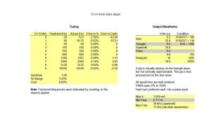 |
Not too shabby at all! The best tuning results I was able to get out of the VCO weren't quite so close - I had a bit of trouble keeping things from going slightly flat at the high end, from around 2400 Hz on up, but at the same time found the VCO to be quite usable with my keyboard and my ribbon controller, and certainly with a sequencer. For the size and very low cost of the circuit, it more than delivers in a number of ways.
In fact, this would be a great VCO to incorporate in many projects - I think it would be a great application to put a couple of these together in a stand-alone portable synth. The exponential control makes it easily controllable with either a pot or a ribbon controller, and provides the ability to patch in that all-important vibrato effect. In any event, I invite you to try this circuit out. You may very well find it's just the circuit you were looking for in that particular application....
Sound Samples
Describing the functions and characteristics of the X-4046 VCO is well and good, but nothing beats actually getting a taste of what it sounds like, so I've prepared a sound sample that covers a number of the features of the VCO. Bearing in mind that the sample itself falls somewhat short of being an artistic masterpiece (just barely), I would never have believed a 4046 IC plus a few other components could ever have produced the sounds featured in the sample.
First of all, I should state that two X-4046 VCOs were used in a couple of portions of this sample. The main sequence heard throughout was the result of one X-4046 VCO modulating the other X-4046 VCO at an audio rate via the linear modulation input (DC coupled in this case). The triangle out of the modulating VCO was modulating the carrier VCO, and the sine output of the carrier through my transistor 2040 filter is what forms the background sequence. Two X-4046 VCOs are also used to form the sync voices heard in the sample. In this case, on X4046 is supplying the sync signal via its pulse output, and the triangle output of the synchronized X-4046 VCO is heard.
Other than the filter, a touch of spring reverb from my Sidekick Amplifier, EG and LFOs used to modulate the frequency and PWM, this sample is made up entirely of the X-4046 VCO. Each waveform output, as well as the hard sync function, is featured. My Thomas Henry keyboard is used to control the VCO(s) (the Klee Sequencer is providing the signals controlling the backing sequence). I play the same series of notes, at differing octaves with each waveform output. The vibrato is supplied by an LFO patched into the keyboard. To vary the sync effect, I manually varied the coarse frequency of the synced VCO as I play the notes.
00:00 The sample begins with the sequenced X-4046 FM patch.
00:41 The PWM output, modulated by a sine LFO, is heard.
01:18 The Rampoid output, set to around the 50% setting is heard.
01:54 The sine output, with a touch of portamento is heard.
02:30 The sawtooth output is heard.
03:01 The triangle output is heard.
03:44 The triangle output, synced to a second X-4046 VCO is heard.
Fadeout: A bit more of the synced triangle wave is heard.
I've supplied an additional sound sample that focuses on the rampoid output.
The rampoid output is a continuously variable waveform that transforms from a triangle wave to a sawtooth wave of twice the frequency of the triangle wave. The Skew control provides the means to vary the waveform through any point between the waveforms.
This sound sample has two sections. It begins with a sequence of notes taken from the Rampoid output; as the sequence progresses, I vary the Skew control. In the second section, I control the X-4046 VCO with the keyboard and play a series of pentatonic notes, adjust the skew control, play another series of pentatonic notes, adjust the skew control again, and so forth.
X-4046 VCO Schematics
The X-4046 schematics are compiled into a single zip archive and linked below.
 |
PCB Layout
After this page was posted, sans PCB layout, Ryk John Miller Thekreator graciously designed a PCB layout for the X-4046 VCO and posted it to this thread on electro-music.com.
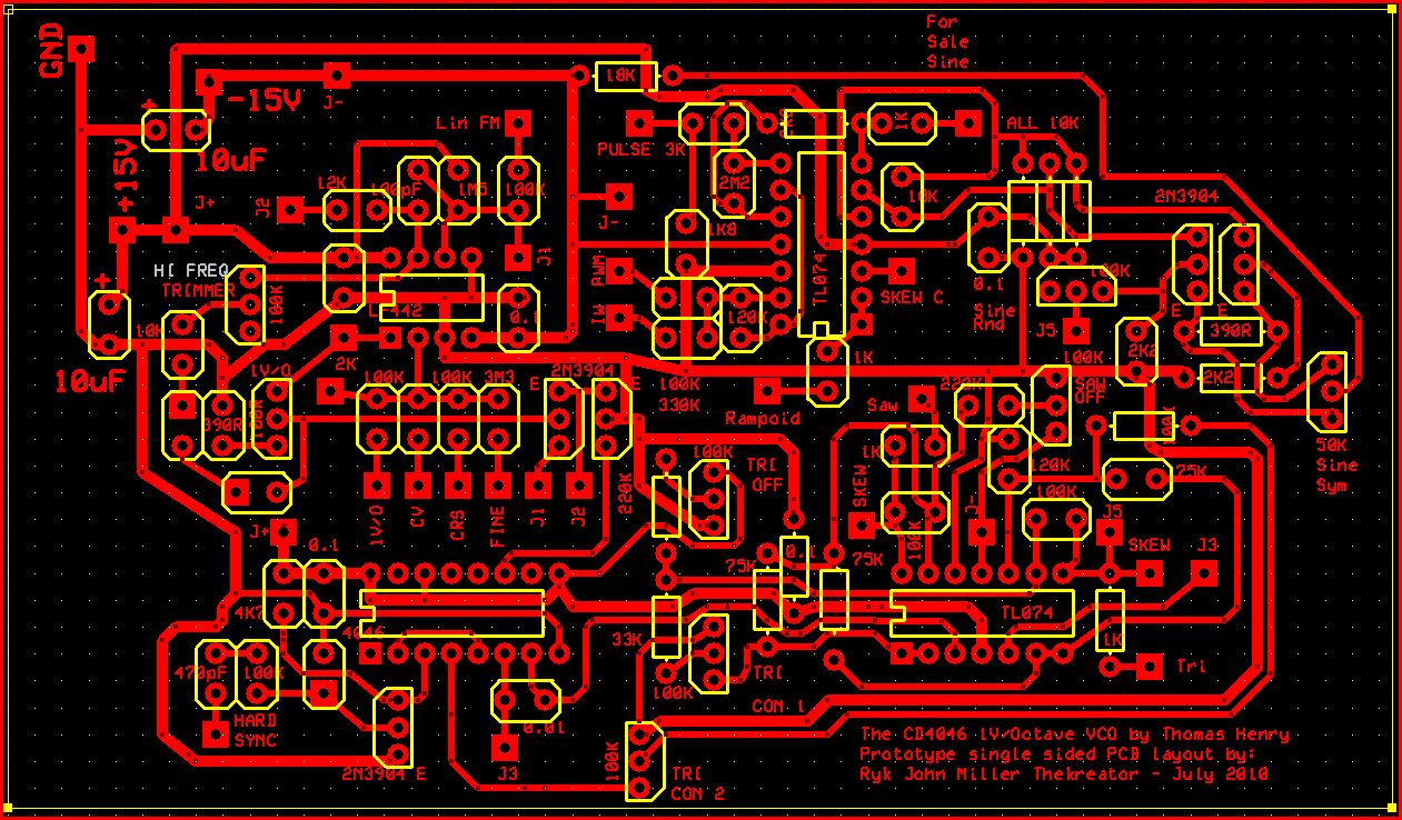 |
All part values are labelled on the PCB with copper! There are not any part #'s placed on the board, as I try to keep everything as compact as I'm able to, with single sided PCBs. (I don't make double or greater, sided PCBs. I can't afford to.)
This PCB is single sided, meant for all of the holes to be drilled.
A DIODE's direction is shown with 2 different solder tabs: The square one is the forward end / line, of the 1N4148
There are 2 different 1/4 watt resistor mounting types. The ones with the holes very close together are meant to be standing upright. The ones with the holes spaced farther apart, are meant to be flush with the PCB.
Each 2N3904 transistor mounting, is your standard flush, TO-92 casing styling, with the Emitter pin (left most on the casing, with the flat portion of it facing you) marked as E.
To determine which pin of each chip is Pin 1 - look to the lower left, of the chip mounting, from it's part # which is mounted below where the chip socket will be placed. Please be very careful with this, if you make this PCB yourself.
Dammit. I JUST realized that I did NOT mark out the Positive pins for the 10uF caps at the power INPUTs to the PCB. Please make sure they're oriented properly.
I tried giving the proper names for each of the trimmers on the PCB. (I myself, usually use 10 to 20 turn trimmers, for any VCO applications - for the greater degree of resistance setting accuracies.)
All of the points where wires are coming to the boards, have SQUARE solder pads, to accept the wiring through
The 3 points for the SLEW panel control, also have square solder pads. The CENTER one is marked as SLEW C.
I tried to place the resistor and capacitor values as close to each of their mounts as possible, so as not to confuse anyone with them
Frequency Control
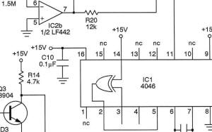
Taking a look at page 1 of the schematic, one thing immediately jumps out: the X-4046 VCO does not control the 4046 VCO frequency through the standard control voltage input at pin 9 of the CD4046. Instead, pin 9 is tied high and an exponential current mirror consisting of Q1 and Q2 is used to provide a variable current source to pin 11 of the CD4046.
This trick allows the VCO to be controlled exponentially rather than linearly. In a "normal" CD4046 application, a resistor (referred to as R1) is connected from pin 11 to ground; the value of this resistor is used in conjunction with the value of the timing capacitor (C), connected between pins 6 and 7, to set the operating frequency range of the VCO when it is controlled by a voltage applied to pin 9. An optional, additional resistor (referred to as R2) with a resistance equal to or greater than R1 can optionally be connected from pin 12 to ground to offset the base operating frequency range that is set by R1 and C. This resistor can be excluded when an offset is not required.
What this tells us is that the current draw at pin 11 plays a role in controlling the frequency of the VCO just as surely as the control voltage input. By tying the control voltage high and instead dynamically controlling the current drawn through pin 11 with a transistor pair, the control of the oscillator can be transformed from the normally linear curve of the voltage input to the exponential curve provided by the current mirror and associated circuitry.
In fact, the control input is virtually identical to any number of VCOs. Present is the transistor pair and accompanying tempco resistor, the volts-per-octave control and modulation inputs, and the linear modulation input.
Waveform Circuitry
Providing a means to control the frequency of the X-4046 exponentially is really only half the battle. If the VCO could only produce the pulse wave output the 4046 VCO normally produces, that would be fair enough, but would ultimately be a limitation in the usefulness of the VCO. This is a fact that was not overlooked by Thomas; in fact, his approach to obtaining the VCO waveforms turns out to be just as "non-standard" as the control scheme he cooked up.
A standard 4046 implementation provides the VCO pulse waveform output at at pin 4. Looking cursorily at page 1, it can be seen that the signal at pin 4 is indeed used, but turning page 2 of the schematic we find that it is only used in conjunction with producing the waveforms a 4046 cannot, in itself, provide. In fact, on page 1, one might also notice that pins 6 and 7 not only provide the standard connections for the VCO timing capacitor, but also connect to points elsewhere in the circuit.
Page 2 of the schematic reveals the mechanics of producing the five waveform outputs of the X-4046 VCO. Here we see that the "normal" VCO output of the 4046 connects directly to a trimpot labeled "Triangle Connect 2", and that timing capacitor pins 6 and 7 actually connect to two sections of a TL074 quad op amp, each of which is configured as a non-inverting buffer/voltage follower. This portion of the schematic reveals how one can use the signals present in a simple 4046 application to produce a number of standard musical VCO waveforms.
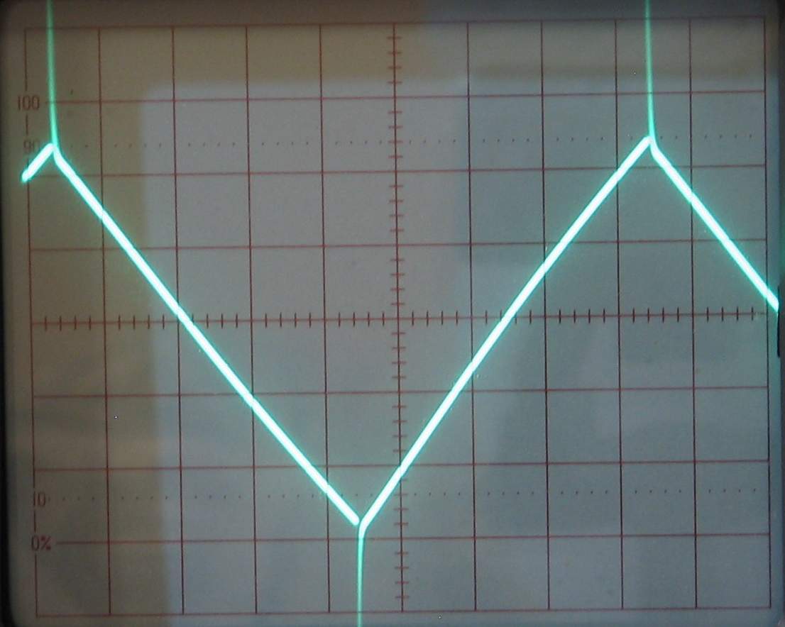
Forming The Triangle Wave
The circuit takes advantage of the timing waveforms present at pins 6 and 7. During the time that the pulse output from pin 4 is high, the signal at pin 7 rises smoothly from 0V to a positive voltage, forming a sawtooth waveform. The signal remains at 0V during the time the 4046 VCO pulse output from pin 4 is low. Likewise, during the time that the pulse output of pin 4 is low, the voltage at pin 6 rises smoothly from zero volts to a positive voltage, again forming a sawtooth waveform. This signal remains at 0V while the voltage at pin 4 is high.
These two voltages are buffered by IC3a and IC3b so that the waveforming circuitry does not load down the operation of the CD4046, which would affect the frequency response of the IC. These two signals are differentially summed by IC3c. Pin 7 is applied to the inverting input of IC3c causing the output of IC3c to produce a falling waveform while the pulse output is high. Because the output is inverted, the voltage, without some sort of offset being applied, would now drop from 0V to a negative voltage.
 |
The needed offset is supplied by the 4046 VCO output at pin 4. This pulse signal is applied, through the Triangle Connect 2 trimpot to the positive input of IC3c. While the inverted pin 7 voltage is dropping, the output at pin 4 is high, providing a push "up" so that the voltage no longer is falling from zero volts to some lower negative voltage; it can now be adjusted up at the right time to connect with the voltage originating from pin 6 of the 4046.
When the VCO output at pin 4 is low, the rising voltage at pin 6 is applied to the noninverting input of IC3c, which maintains the rise in voltage at the output of IC3c.
The result of all this is that a sloped rising and a sloped falling voltage is made available for every cycle of the 4046 VCO. These two waveforms are joined together by "pushing" the falling voltage up with the Triangle Connect 2 adjustment and by adjusting the "size" of this voltage so that it matches the voltage from pin 6. This connects the two ends of the two sloped waveforms to form a triangle wave for each cycle of pulse wave produced by the 4046 VCO. After joining the ends together, the Triangle Offset adjustment is used to center the composite waveform around zero volts.
The process of joining the two waveforms together does result in pips at the connection points; these pips carry over into the sawtooth and rampoid waves, though they are smoothed considerably on the sine output. Though these pips dirty up the appearance of the waveforms, audibly they work just fine. Even the early Moog waveforms had interesting measurable non-linearities in them, but were certainly musically viable.
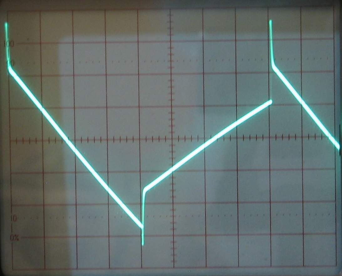
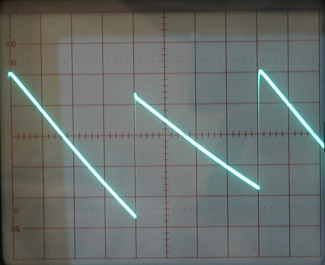
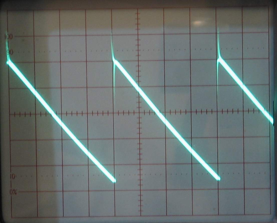
Forming the Sawtooth Wave
As mentioned before, the voltage at pin 6 is rising while the signal at pin 7 is resting at zero volts, and the voltage at pin 7 is rising while the signal at pin 6 is at zero volts.
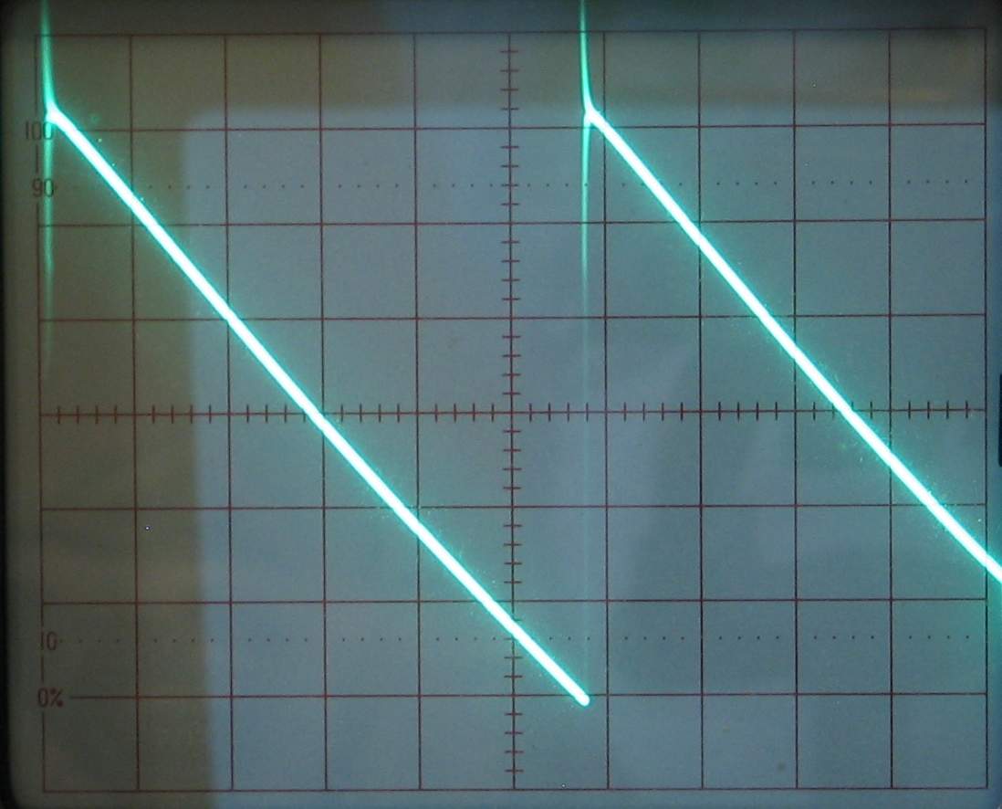 |
By combining these two signals together at IC3d, a composite sawtooth wave is formed at twice the frequency of the 4046 VCO: for each cycle of the pulse wave, there are two cycles of sawtooth wave. The Saw Offset adjustment is used to center the sawtooth output around zero volts.
Forming the Rampoid Wave
Once the triangle and sawtooth waves have been formed, it's a simple matter to produce the rampoid wave.
The triangle waveform is connected to one end of the Skew control and the sawtooth wave is connected to the other end of the Skew control. The center tap of the Skew control is applied to IC4a, which is configured as a buffer/voltage follower.
 |
 | |  |
| 25% Skew | 50% Skew | 75% Skew |
 |
By adjusting the Skew control, the balance of these two waveforms can be continuously adjusted to form the Rampoid output. This is a marvelous function, particularly in the fact that the sawtooth waveform is always one octave above the triangle waveform. The ability to continuously vary the balance of these waveforms provides a marvelous means to vary the timbre of this output.
Forming the Sine Wave
Anyone familiar with Thomas' previous work will immediately identify this section. This circuit is used in a number of Thomas' past designs; it is a sublime sine shaping circuit that doesn't use anything more than an op amp, a couple of transistors, some resistors and a couple of trimmers.
 |
Once the triangle wave is derived from the circuit, it's merely another step (this section) to produce a very nice sine wave.
Forming the Pulse Wave/PWM Output
Once the more exotic wave manipulation of deriving first a triangle and then a sine wave from the 4046 has been accomplished, a more versatile pulse wave output can be formed.
 |
The CD4046 VCO does produce a fixed pulse output, but the waveform generated by this section of the circuit is far more versatile in that the duty cycle of the pulse wave can be adjusted manually with the Initial Width control and modulated through the PWM input. This section of the circuit again employs a standard method of deriving the pulse output from the sine wave. The sine wave is sent to a comparator formed by IC4c and R55; the Initial Width control signal and any signal applied to PWM input are summed together by IC4d and applied as the reference to that comparator. Thus variation of the combined pulse width control signal will change the reference signal to the comparator and alter the point at which the sine wave will trip the comparator high and low.
Hard Sync
The CD4046 Phase Comparator 1 contains an exclusive OR gate and the internal VCO of the CD4046 has an integral inhibit function, which is controlled through pin 5. When pin 5 is held high, the VCO is prevented from operating. This design uses both of these features to produce an exquisite hard sync function.
On page 1 of the schematic, note that the output of the XOR gate (pin 2) is connected directly to the inhibit pin of the CD4046 (pin 5). One input of the XOR gate (pin 14) is held high. This essentially configures the XOR gate as an inverting buffer.
The second input to the XOR gate (pin 3) is connected to the collector of Q3. With no signal applied to the hard sync input, the collector of Q3 is held high by the voltage applied through R14. Because the XOR gate is configured as an inverting buffer, the output of the XOR gate (pin 2) is held at a constant low as long as no sync signal is applied to the hard sync input. This low signal allows the VCO to operate without interruption by holding pin 5 low.
When a pulse signal is applied to the Hard Sync input, C2 will convert each positive-going transistion of the applied pulse signal into a narrow positive pulse. Each of these pulses will cause the voltage on the collector of Q3 to briefly be pulled low. Each time the Q3 collector voltage is pulled low, the output of the XOR gate is pulled high, and each time the output of the XOR gate is pulled high, the VCO is reset, resulting in the hard sync effect.
Miscellaneous Circuit Notes
While breadboarding this circuit, I had a number of "brands" and vintages of 4046 ICs on hand to test. At least with my setup, I found that particular 4046s seemed much more difficult to tune to a standard V/Oct response at any frequency. In fact, I found that some 4046 devices would not "make it out of the gate" so to speak. These particular ICs were the Texas instrument CD4046BE; they would not even make the first octave from 80 to 160 Hz. To confirm that I just didn't have a "bad" batch I'd picked up at a surplus house, I ordered more of them through Mouser Electronics, but this batch acted just as badly. To triple check, I sent Thomas some of the original TI chips and he confirmed that that particular brand just would not conform to the results he was obtaining from the National part that he used in his circuit.
There was one other type of 4046 that did not quite make the grade (in comparison to others that seemed much easier to tune) and that was the SGS Microelectronics HCF4046. Note that I don't consider these ICs to be inferior in any way for their intended original application, but judging solely from my experience, they certainly seem to have a slight bit of difference in die or manufacturing process that makes them less compatible with this design.
Knowing next to nothing of the actual internal differences, and from what I can tell by reviewing a number of different CD4046 datasheets, the specification that seems be the most predictive as to how closely a 4046 will follow a voltage input on a volts-per-octave basis is listed in the specifications as "VCO Linearity". Chances are if you base the selection of the 4046 you intend to use on this specification, you may have an easier time of producing quite respectable results.
The CD4046 ICs that I found to be more compatible with the design would list the following as the VCO linearity specification:
The few CD4046 ICs that I found to be less compatible with the design did coincidentally list the following as the linearity specification:
VCO In= 7.5V, +/-5V, R1 = 1M: Linearity = 7%
The particular brands of CD4046 I found to tune more easily/consistently are as follows:
Fairchild CD4046
Motorola MC14046
My favorite of all of them was the Motorla MC14046; Thomas used a National part. The age of the IC did not seem to matter. Note that this is my own experience and conjecture of course; if you have a stack of CD4046s, take a look at what you have, and see if you have a spec sheet for it. If all else fails, just insert what you have - it may just work fine for you, too.
The transistor pair consists of a couple of 2N3904s. These transistors can be matched, if you choose. Thomas' results were actually obtained with a pair of transistors that had not been matched, though they had been physically bonded together. If you choose, even a matched package (such as an LM394) can be used. For stable frequency operation over temperature, be sure to situate the tempco resistor so that it is in contact with the transistor pair. For non-critical applications, the tempco resistor (R9) can be substituted with a 2K metal film resistor.
Calibration
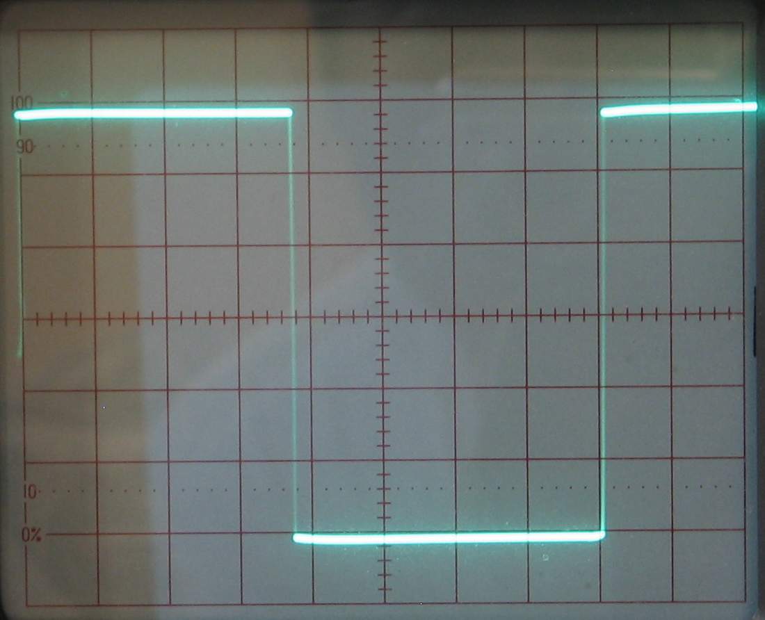
There are a number of trimpots in this circuit. Generally, to calibrate the waveforms themselves, an oscillocope will come in extremely handy, but the frequency trim can be done by ear, or by ear with a frequency counter to help guide you along the path.
First of all, you will want to adjust the triangle wave output so that it is generating a triangle wave centered around 0V. Connect the triangle wave output to an oscilloscope, DC coupled, and observe the waveform on the oscilloscope. Depending on the intial settings of the trimpots, you will likely see a waveform that does not represent a triangle wave at all, but you should see a rising voltage and a falling voltage.
Use the coarse and fine adjustments of the VCO to set the waveform you do see to around 1 kHz.
Adjust R37 (Triangle Connect 1) and R39 (Triangle Connect 2) so that the rising and falling waveforms connect together to form a triangle wave. You may see some pronounced pips, though by ear the triangle will sound pretty good. You may need to adjust R38 (Triangle Offset) so that the two waveforms fall around the 0V point as you connect the two waveforms together, and, ultimately, once the two waveforms are connected together, you will want to use R38 to center the triangle wave around 0V. Ultimately, you will come up with a 10Vp-p triangle waveform, centered around 0V.
Once the triangle waveform is calibrated, connect the Saw output to the oscilloscope and adjust R40 (Saw Offset) so that the sawtooth waveform is also centered around 0V.
Connect the Sine output to the oscilloscope and adjust R21 (Sine Symmetry) and R41 (Sine Round) so that a reasonable sine waveform is present on the sine output. As always, this adjustment may take a few trips between the two pots until you have a satisfactory sine waveform. If possible, it helps to output this waveform to a speaker (but don't connect directly to an amplifier - this is a 10Vp-p hot signal) so that it sounds as pure as possible to your ears, which are, of course, the most accurate measuring instruments you possess.
The calibration of the X-4046 frequency tuning is best explained by Thomas, which is fortunate for you, dear reader. I took a stab at writing a coherent version, but I couldn't quite nail it like Thomas himself:
Begin by making sure the high frequency trimmer is set to maximum resistance. If you need to, pull it out of the circuit and confirm that it's full-up with a multimeter. In any event, in what follows, you don't want to use it in a heavy-handed fashion. Typically, just the smallest amount of HF injection is needed to fix things up around 10KHz or so. In fact, many people won't need to touch this trimmer at all depending on component tolerances, layout techniques and their Zodiac sun-sign.
Next let the VCO warm up for an hour or so, and any test equipment as well. We might as well rule out any burn-in drift.
Now tune the VCO completely by ear. That is, while playing octaves, set the volt-per-octave trimmer to give the best possible results. Since you're probably using a multiturn unit, it's important to rough things in by ear before pulling out the test instruments. Some builders may wish to stop here depending on their accuracy requirements. If the goal is simply to play lead lines (no tracking harmonies, etc.) then what could be better than having a VCO that *sounds* in tune! The same thing applies to users who are controlling this with a ribbon or other non-keyboard controller. I mean, if your ears can't tell the difference, then who cares what the frequency counter says?
For more detailed tuning, continue by hooking up a frequency counter. I also use the 1V stepper I published in the VCO Chip Cookbook, but you could use a standard keyboard to provide the voltages. I usually connect a DVM to the voltage source as well, to confirm that I'm really getting 1V increments. By the way, the frequency counter I use also appeared in the book just mentioned.
Now while watching the counter, tune the circuit perfectly for 80Hz to 160Hz. I was able to make this dead on (at least to the limit of my homebrew frequency counter with a 1 second gate), and so should others. Now check 160Hz to 320Hz. If there's any discrepancy, adjust the trimmer accordingly. Now go back and confirm 80Hz to 160Hz again. It shouldn't have changed much if at all, otherwise split the difference and check with 160Hz to 320Hz again.
Now jump to 320Hz to 640Hz. I've usually noticed a certain variation at this point (which then disappears in the next octave), so don't go too wild with the trimmer. Once you're up this high, the cents deviation from perfect tuning becomes less noticeable, naturally. Just try to keep within 1 Hertz of 640.
A person should be able to get up to 1280Hz without too much deviation. Keep checking two consecutive octaves at a time, and try to spread out any noticeable error.
When going to octave 5120Hz, if you are wildly flat, then start to very gently ease in some of the HF trim. Once you've done so, however, be sure to check the lower octaves starting the process over with 80Hz as before. Be prepared to go around the horn here numerous times.
Finally, at 10240Hz, boost the HF once again if needed. Keep in mind that when you jump from 80Hz to 10240Hz, say, or vice-versa you'll need to allow a certain settling time. For whatever reason (probably a trait of CMOS) the frequency CV slew rate is fairly slow.
It usually takes me a couple hours to tune the X-4046 VCO. The entire time I keep a close watch on the DVM to make sure I'm really getting a 1V step between octaves and that temperature drift hasn't affected my voltage stepper (which I can easily recalibrate if need be). As my X-4046 VCO Test Results sheet shows, I was able to tune this fairly well from 80Hz to 10240Hz, although so far two other people have been unable to duplicate my results. I'm either lucky or deaf! But seriously, this VCO is harder to tune than most, the reason being that it doesn't provide perfect tuning throughout its range but requires spreading the errors out to regions where they are least noticeable. Despite this, it has enough going for it to make the extra time spent in tuning worthwhile, I think.